- 您现在的位置:买卖IC网 > Sheet目录323 > EK-K7-KC705-CES-G-J (Xilinx Inc)KINTEX-7 FPGA KC705 EVAL KIT
Kintex-7 FPGAs Data Sheet: DC and AC Switching Characteristics
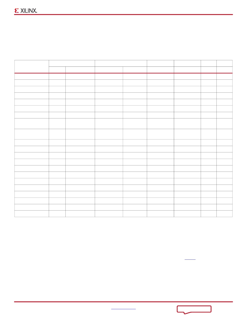
DC Input and Output Levels
Values for V IL and V IH are recommended input voltages. Values for I OL and I OH are guaranteed over the recommended
operating conditions at the V OL and V OH test points. Only selected standards are tested. These are chosen to ensure that
all standards meet their specifications. The selected standards are tested at a minimum V CCO with the respective V OL and
V OH voltage levels shown. Other standards are sample tested.
Table 9: SelectIO DC Input and Output Levels (1)(2)
I/O Standard
V, Min
V IL
V, Max
V, Min
V IH
V, Max
V OL
V, Max
V OH
V, Min
I OL
mA
I OH
mA
HSTL_I
HSTL_I_12
HSTL_I_18
HSTL_II
HSTL_II_18
HSUL_12
LVCMOS12
LVCMOS15,
LVDCI_15
LVCMOS18,
LVDCI_18
LVCMOS25
LVCMOS33
LVTTL
MOBILE_DDR
PCI33_3
–0.300
–0.300
–0.300
–0.300
–0.300
–0.300
–0.300
–0.300
–0.300
–0.300
–0.300
–0.300
–0.300
–0.400
V REF – 0.100
V REF – 0.080
V REF – 0.100
V REF – 0.100
V REF – 0.100
V REF – 0.130
35% V CCO
35% V CCO
35% V CCO
0.700
0.800
0.800
20% V CCO
30% V CCO
V REF + 0.100
V REF + 0.080
V REF + 0.100
V REF + 0.100
V REF + 0.100
V REF + 0.130
65% V CCO
65% V CCO
65% V CCO
1.700
2.000
2.000
80% V CCO
50% V CCO
V CCO + 0.300
V CCO + 0.300
V CCO + 0.300
V CCO + 0.300
V CCO + 0.300
V CCO + 0.300
V CCO + 0.300
V CCO + 0.300
V CCO + 0.300
V CCO + 0.300
3.450
3.450
V CCO + 0.300
V CCO + 0.500
0.400
25% V CCO
0.400
0.400
0.400
20% V CCO
0.400
25% V CCO
0.450
0.400
0.400
0.400
10% V CCO
10% V CCO
V CCO – 0.400
75% V CCO
V CCO – 0.400
V CCO – 0.400
V CCO – 0.400
80% V CCO
V CCO – 0.400
75% V CCO
V CCO – 0.450
V CCO – 0.400
V CCO – 0.400
2.400
90% V CCO
90% V CCO
8
6.3
8
16
16
0.1
0.1
1.5
–8
–6.3
–8
–16
–16
–0.1
–0.1
–0.5
SSTL12
SSTL135
SSTL135_R
SSTL15
SSTL15_R
SSTL18_I
SSTL18_II
–0.300
–0.300
–0.300
–0.300
–0.300
–0.300
–0.300
V REF – 0.100
V REF – 0.090
V REF – 0.090
V REF – 0.100
V REF – 0.100
V REF – 0.125
V REF – 0.125
V REF + 0.100
V REF + 0.090
V REF + 0.090
V REF + 0.100
V REF + 0.100
V REF + 0.125
V REF + 0.125
V CCO + 0.300 V CCO /2 – 0.150 V CCO /2 + 0.150
V CCO + 0.300 V CCO /2 – 0.150 V CCO /2 + 0.150
V CCO + 0.300 V CCO /2 – 0.150 V CCO /2 + 0.150
V CCO + 0.300 V CCO /2 – 0.175 V CCO /2 + 0.175
V CCO + 0.300 V CCO /2 – 0.175 V CCO /2 + 0.175
V CCO + 0.300 V CCO /2 – 0.470 V CCO /2 + 0.470
V CCO + 0.300 V CCO /2 – 0.600 V CCO /2 + 0.600
14.25
13.0
8.9
13.0
8.9
8
13.4
–14.25
–13.0
–8.9
–13.0
–8.9
–8
–13.4
Notes:
1.
2.
3.
4.
5.
6.
7.
8.
Tested according to relevant specifications.
3.3V and 2.5V standards are only supported in 3.3V I/O banks.
Supported drive strengths of 2, 4, 6, or 8 mA in HP I/O banks and 4, 8, or 12 mA in HR I/O banks.
Supported drive strengths of 2, 4, 6, 8, 12, or 16 mA in HP I/O banks and 4, 8, 12, or 16 mA in HR I/O banks.
Supported drive strengths of 2, 4, 6, 8, 12, or 16 mA in HP I/O banks and 4, 8, 12, 16, or 24 mA in HR I/O banks.
Supported drive strengths of 4, 8, 12, or 16 mA
Supported drive strengths of 4, 8, 12, 16, or 24 mA
For detailed interface specific DC voltage levels, see the 7 Series FPGAs SelectIO Resources User Guide ( UG471 ).
DS182 (v2.8) March 4, 2014
Product Specification
8
发布紧急采购,3分钟左右您将得到回复。
相关PDF资料
EK-S6-SP601-G
KIT EVAL SPARTAN 6 SP601
EK-S6-SP605-G
KIT EVAL SPARTAN 6 SP605
EK-V6-ML631-G-J
VIRTEX-6 HXT FPGA ML631 EVAL KIT
EK-V7-VC707-CES-G
VIRTEX-7 VC707 EVAL KIT
EK-Z7-ZC702-CES-G
ZYNQ-7000 EPP ZC702 EVAL KIT
EL1848IYZ-T7
IC LED DRIVR WHITE BCKLGT 8-MSOP
EL7156CSZ
IC DRIVER PIN 40MHZ 3STATE 8SOIC
EL7158ISZ
IC DVR PIN 40MHZ 3STATE 8-SOIC
相关代理商/技术参数
EK-K7-KC705-G
制造商:Xilinx 功能描述:KINTEX-7 FPGA KC705 EVALUATION KIT 制造商:Xilinx 功能描述:KINTEX-7 FPGA KC705 EVALUATION KIT - Boxed Product (Development Kits) 制造商:Xilinx 功能描述:KINTEX-7 FPGA KC705 EVAL KIT
EK-K7-KC705-G-J
制造商:Xilinx 功能描述:KINTEX-7 FPGA KC705 EVAL KIT
EKK8011
制造商:未知厂家 制造商全称:未知厂家 功能描述:USB + PS/2 keyboard controller
EKK8011AB
制造商:EMC 制造商全称:ELAN Microelectronics Corp 功能描述:USB & PS/2 Keyboard Encoder
EKK8301
制造商:未知厂家 制造商全称:未知厂家 功能描述:PS/2 keyboard controller
EKK-EVALBOT
功能描述:开发板和工具包 - ARM Keil Stellaris Eval Robot
RoHS:否 制造商:Arduino 产品:Development Boards 工具用于评估:ATSAM3X8EA-AU 核心:ARM Cortex M3 接口类型:DAC, ICSP, JTAG, UART, USB 工作电源电压:3.3 V
EKK-LM3S1968
功能描述:开发板和工具包 - ARM Stellaris Eval Kit w/ ARM/Keil Tools RoHS:否 制造商:Arduino 产品:Development Boards 工具用于评估:ATSAM3X8EA-AU 核心:ARM Cortex M3 接口类型:DAC, ICSP, JTAG, UART, USB 工作电源电压:3.3 V
EKK-LM3S1968
制造商:Texas Instruments 功能描述:LM3S1968 MCU Eval Kit w/ Keil RealView M
